
Dielectric Constant(DK)
If you’ve ever played with a prism as a child, then you’re likely aware of how it can be used to split white light into its constituent colors and how it bends light that passes through it. These are fundamental experiments that any student will need to perform and understand as they prepare for a career in science and engineering.
One aspect of PCB substrate materials that can often be overlooked by PCB designers is the effect of the substrate dielectric constant on signal integrity in a PCB.
Dispersion is present in any material, and this can distort digital signals, especially when a device switches at very high speeds. Designers need to consider the tradeoff between cost, performance, and other material properties when choosing the appropriate substrate for their next device.
Should You Use High-k or Low-k PCB Substrate Materials?
Answering this question is really about considering the tradeoff between dielectric constant and other PCB substrate material properties. Some PCB substrate materials, such as Rogers high speed laminates or other ceramic materials, have more desirable optical properties but carry higher costs. These other materials can be more difficult to work with in a manufacturing process, thus they also carry higher fabrication costs. Certain PCB substrate materials are better for working with RF circuits and components and may be the best choice for mission critical applications that operate at extremely high speeds and high frequencies.
While we normally consider the imaginary part of the dielectric constant, the real part (i.e., the refractive index) is also important from a layout standpoint. The real part of the dielectric constant determines the speed at which an electromagnetic wave propagates through a material, while the imaginary part determines gain or loss in the material as the wave propagates. In terms of PCB design, the dielectric constant and trace geometry will determine how a signal propagates along a trace.
Standard FR4 substrates have a dielectric constant of ~4.5, although the weave pattern used in the substrate will affect the exact value of the dielectric constant. The dielectric constant of ceramic-filled PTFE substrates can be tuned from ~3 to ~10 and losses can be reduced by an order of magnitude by using different fillers and bonding materials. The effect of tuning on dispersion in PCB substrate materials varies, although the best materials manufacturers will have this data on hand for use by designers.
Real Part: Propagation Delay and Impedance
If you remember your physics 101 classes, then you know that the refractive index (i.e., the square root of the real part of the dielectric constant) determines the speed at which an electromagnetic wave propagates through a material. The speed of a signal on a trace depends on the effective dielectric constant, which is determined by the geometry of the trace and the dielectric constant of the PCB substrate material.
Note that, for a given substrate material, a stripline will have a larger effective dielectric constant than a microstrip. If you look at the equations for the impedance of microstrips and striplines, it is implied that you should not include the imaginary part of the dielectric constant in the characteristic impedance calculation. Instead, the impedance is only determined by the real part of the substrate dielectric constant and the trace geometry.
The speed of signals on a trace affects the transition to transmission line behavior. With longer traces, the propagation time for a signal is longer. The critical threshold for considering transmission line effects and the requirements for impedance matching and termination is that the propagation delay is greater than ~35% of the signal rise time.
Imaginary Part: Loss Tangent, Parasitics, and Losses
The imaginary part of the dielectric constant (also called the dissipation factor or loss tangent) determines the losses a signal sees as it travels through a trace. In total, there are three major sources of loss on a trace carrying an electromagnetic wave:
1, Dielectric losses: this occurs due to the magnitude and phase of an induced polarization wave in the PCB substrate material. This is related to the imaginary part of the dielectric constant, which is proportional to the conductivity of the substrate.
2, Resistive heating in a trace: some electromagnetic energy is converted to heat due to the sheet resistance in the trace. Note that the sheet resistance of a trace can be quite large at high frequencies due to the skin effect.
3, Parasitics: the substrate has some residual conductance, which allows some current in a signal to pass to the return line. The real part of the substrate dielectric constant also determines the parasitic capacitance. These two terms together determine the loss tangent.
Three other sources of loss that are generally not considered are
1,Insertion loss: this is important in transmission lines and is related to the characteristic impedance, signal frequency, trace geometry, and effective dielectric constant.
2,Radiation losses: any oscillating current will emit an electromagnetic wave, which carries energy away from the circuit.
3,Roughness of the conductor: the electromagnetic field will concentrate near the rough edges of a conductor, leading to greater resistive losses in these regions.
Transmission line models and impedance models for traces in a PCB often omit the imaginary part of the dielectric constant, but the geometry of traces and embedding in the PCB substrate material will affect losses by changing the effective dielectric constant (both real and imaginary parts).
Signals on microstrips incur lower losses than signals on striplines because stripline traces are surrounded by the dielectric. This is because the wave travels partially through the dielectric around a trace and will experience dielectric losses from the substrate. These waves will couple back into the trace due to continuity at the interface between the conductor and PCB substrate material, which determines the losses as a signal is guided along the conductor. When considered alongside resistive heating, this addresses the first two points above.
When considered alongside the real part of the dielectric constant, the parasitic capacitance and conductivity of the substrate, which are respectively related to the real and imaginary parts, determine the loss tangent. This can be summarized in the following formula: 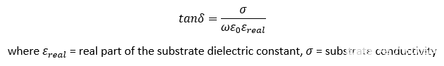
One can initially conclude that devices produced with lower volume and that must maintain signal integrity at very high speeds or frequencies should use a material with lower losses. Using a lower dielectric constant is beneficial from a propagation delay standpoint, although it has mixed effects on the characteristic impedance of traces and transmission lines in your PCB. Careful modeling is required to determine an acceptable range of the real and imaginary parts of the dielectric constant for your next high speed or high frequency system.
Diagnosing signal integrity problems can be tricky as your designs become more complex, and properly modeling the dielectric constant of PCB substrate materials. The powerful signal integrity and power integrity tools in the Sigrity Broadband SPICE package provides designers with the tools they need to diagnose the effects of dielectric constant on signal integrity in high speed and high frequency systems. This unique tool considers a range of IC packages for use in a variety of circuit analyses.
